
What are System-in-Packages?
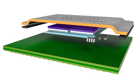
A system-in-package or system-in-a-package (SiP) is a semiconductor circuit which combines several chips in a single package resulting a complete electronic system. The primary features of SiPs are the relatively low assembly costs and the space savings that can be achieved, since different chips can be stacked on top of each other into a package and interconnected via wire bonding or through-silicon vias. The integrated components are attached to a substrate (e.g. FR4) and protected from external influences by a coating or molding.
The SiP itself combines all or at least most of the functionalities of the individual electronic systems in one package.
Applications of System-in-Packages
Due to the many advantages of system-in-packages such as their compactness and cost efficiency along with the general market trend towards continuously smaller minaturized systems, the importance of this technology is becoming more and more significant. Specific use cases across industries are sensors, circuits, memory modules and actuators - in which each respective microsystem is combined in a single package.
Laser cutting of SiPs
With the laser as a cutting tool and as an attractive alternative to mechanical cutting processes, system-in-package (SiP) can be processed most economically. Laser depaneling offers a number of advantages: firstly, the non-contact process does not induce any mechanical stress in the material. Secondly, the deposition of residues that could trigger malfunctions is avoided due to the process.
LPKF has many years of experience in the field of laser depaneling as well as with regard to the specific requirements of SiP processing and is therefore able to process a very wide range of compositions.
LPKF's laser systems can not only achieve the highest quality requirements, a very high effective cutting speed can be reached as well. The speeds can vary depending on the desired quality of the cut as well as the material thickness and composition of the PCBs. For thicker boards, these tend to be quite a bit lower.
If you are interested in laser depaneling for your SiP applications, please feel free to contact us and send us your samples.
Benefits laser processing of SiPs
Laser depaneling systems from LPKF have outstanding precision that cannot be reproduced by mechanical methods. This is especially important in view of the increasing miniaturization of circuitry as well as the rising demands on quality and the reduction of potential processing errors and associated costs.