
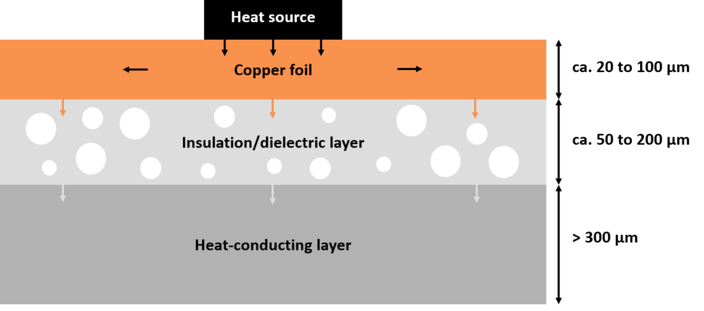
Structure of Insulated Metal Substrates (IMS)
Printed circuit boards with a metal core basically consist of three different layers (see figure):
- Circuit layer: e.g. copper foil
- Dielectric layer: e.g. of polymer or ceramic
- Heat conducting layer: e.g. of aluminium, copper or stainless steel
These layers differ significantly in terms of their respective material thickness. The individual heat conducting layers are characterized by varying thermal conductive coefficients, which qualify the materials for different areas of application.
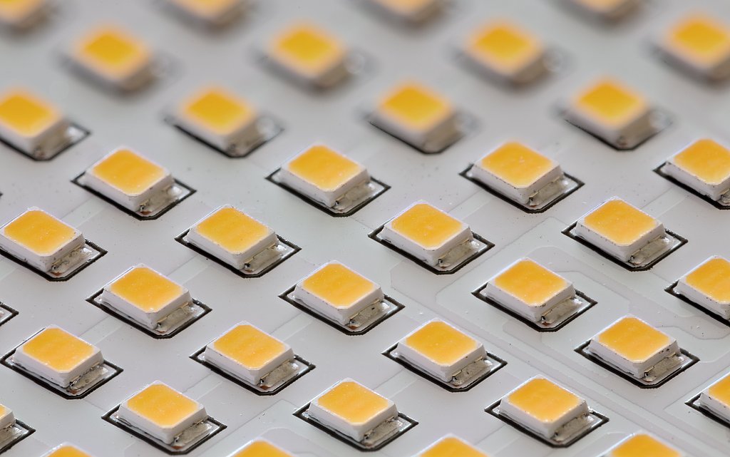
Application of Insulated Metal Substrates (IMS)
Insulated Metal Substrates can be found in a variety of applications, which are especially characterized by increased reqirements for heat dissipation. These include among others:
- Power electronics (e.g. transformers, transistor arrays, motor drivers etc.)
- Automotive/Transport (e.g. light/LED modules, GPS systems, power modules etc.)
- Communication (e.g. power amplifier, transmitters, microstrip circuits etc.)
- Consumer electronics (e.g. motor and voltage regulator, amplifiers, equalizer etc.)
- And much more
Comparison of IMS with Further Circuit Board Materials
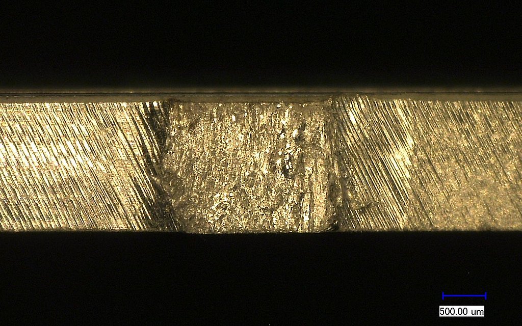
Laser Cutting of IMS PCBs
Using the laser as a cutting tool, Insulated Metal Substrates (IMS) or metal core PCBs can be processed as an highly economical and attractive alternative to mechanical separation processes. Thereby laser depaneling has several advantages: Firstly, the non-contact process does not induce any mechanical stress into the material. On the other hand, the deposition of metal swarfs, which can trigger short circuits, is avoided due to procedural reasons.
LPKF has developed its own solution especially for laser depaneling and the specific requirements of IMS processing, which enables the PCBs to be cut with a powerful laser.
LPKF's laser systems can achieve very fast effective cutting speeds. These can vary depending on the desired quality of the cut and the material thickness and composition of the printed circuit boards. With thicker boards these tend to be lower.
If you are interested in laser depaneling of your IMS applications, please feel free to contact us and send us your samples.
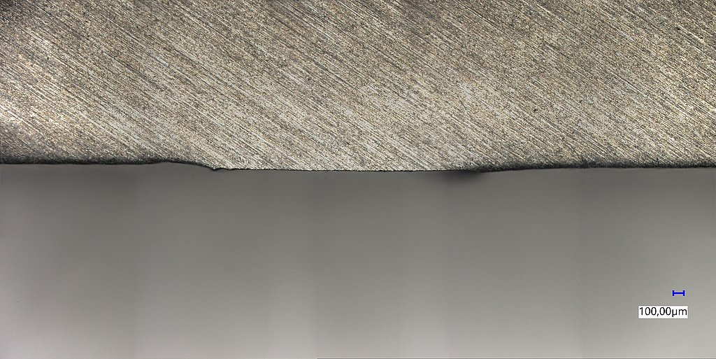
Benefits of laser processing
Cutting printed circuit boards from the panel using a laser offers the user some significant advantages over mechanical cutting processes:
Comparison with other separation processes of IMS
In contrary to mechanical processes, such as milling, no dust or swarf is formed when cutting out the circuit boards with laser, which could desposit on the the cutting edge or the circuit board itself. Gases and particles that are produced when the material is ablated are removed by a powerful extraction system.